Monday, April 25, 2005

The Multiplier

Having looked at just how large the ROM [and, by implication, the forthcoming RAM] are going to be, suddenly another 350 gates for a dedicated multiplier don't seem so bad. Of course, this one only works for unsigned numbers, but it's not too hard to add in the hardware for signed multiplication as well. I'll either do that by sign-extending the inputs or by something slightly more complex, but I don't quite have time to manage it tonight.

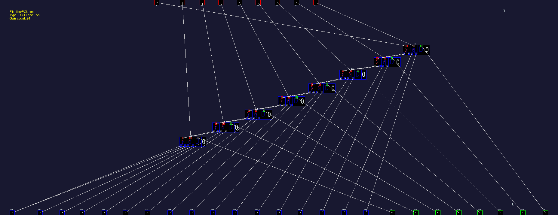
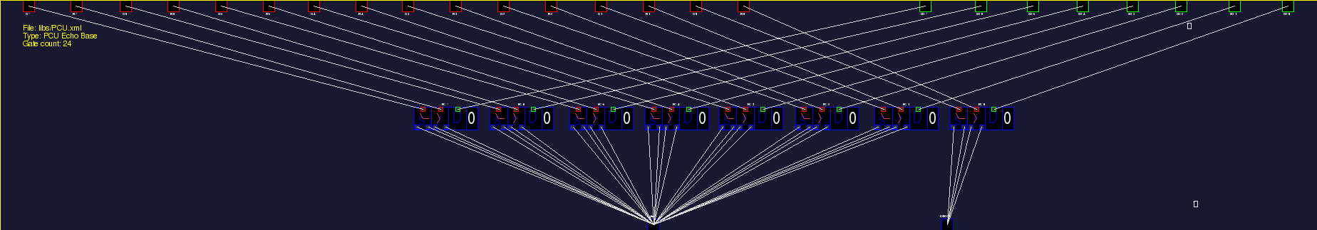
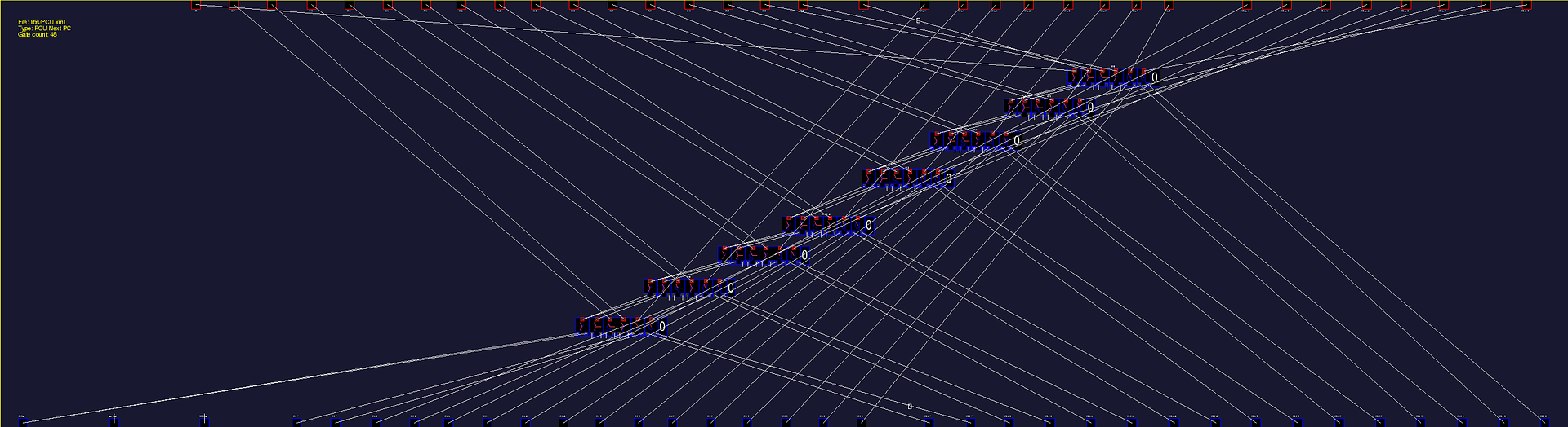
You will note [and I use the word will rather speculatively, I realize] that the multiplier is a bit more complex than it needs to be. The accumulator is obvious and minimal, but the circuits that feed into it are actually optimized for speed. I could just have done the simple 64-ball-paths crossbar of the 8 bits of each input. That would always have completed its calculations in a predictable amount of time [(64 balls) + (arg input, reset, and readout)], but it would often have spent lots of its time multiplying zero by zero. The design I decided to use instead recognizes zeroes in Op0 and skips all processing [including state machine reset] on those bits. Of course, the state machines used to do that recognition aren't free. The processing time is (10 balls per bit) + (the other stuff). That gives us a worst case [multiplying by -1] of (80 balls) + (all the other stuff), but that'll be quite rare. It's made rarer still by the fact that any constant -1 multiplications can just be replaced by complements, which should be significantly faster.

[Image] Multiplier Test

Click on the yellow boxes to see inside them.


[Image] Multiplier

Click on the yellow boxes to see inside them.


[Image] 1 to 16

Click on the yellow boxes to see inside them.


Sunday, April 10, 2005

The Program Counter Unit

If the ALU is the heart of the CPU, then the PCU is surely the bit that nags you to get off your ass and do things. Wait--no--maybe it's the brain. Yeah, that's probably it.

It's a bit awkward for me to try to abstract out a monolithic PCU block for testing. At least in my design, the PCU is quite closely tied in to the master state machine that controls the entire CPU. What I've ended with up here is therefore not a box labelled "PCU" that you just hook up to your ROM, RAM, ALU, etc. It's a set of pieces:
In this test I'm just displaying the link register's value rather than actually using it, and my opcodes are just:
  • nop
  • branch to immediate value
  • branch-and-link to immediate value
In order to have a complete view of all sorts of different branching instructions, well...I'd have to have done a lot more work. I'll get there, but for today at least I've tested all the basic parts I'll need.

Incidentally, the two small text boxes in the screen shot, which are probably too small to read, contain the following text:

Phases of operation:

   Read Next PC->PC
   Increment PC
   Read PC->ROM
   Process instruction

Opcodes for this test [bits 15-14 only]:

   0x0000: No-op
   0x4000: No-op
   0x8000: branch to addr in bits 13-6
   0xC000: branch-and-link to addr in 13-6

[Image] PCU Test

Click on the yellow boxes to see inside them.


[Image] 1 to 16 Triggered

Click on the yellow boxes to see inside them.